
R&D for next-generation precision part solutions in semiconductor wet-clean processes
Advanced R&D Solutions for Semiconductor Parts
HS HI-TECH
Custom precision machining solutions for higher yield. Proven OEM, ODM and reverse engineering capability makes us the partner that maximises the reliability of semiconductor equipment parts.
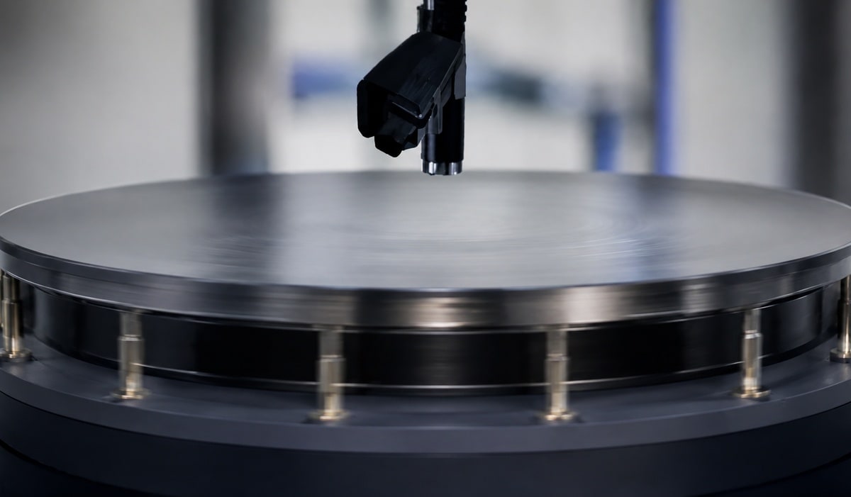
Precision wafer rotation technology
Chemical, heat and cleanliness are designed and built in house. We were the first in the industry to apply insert moulding, holding form and precision even under rotation.
See the products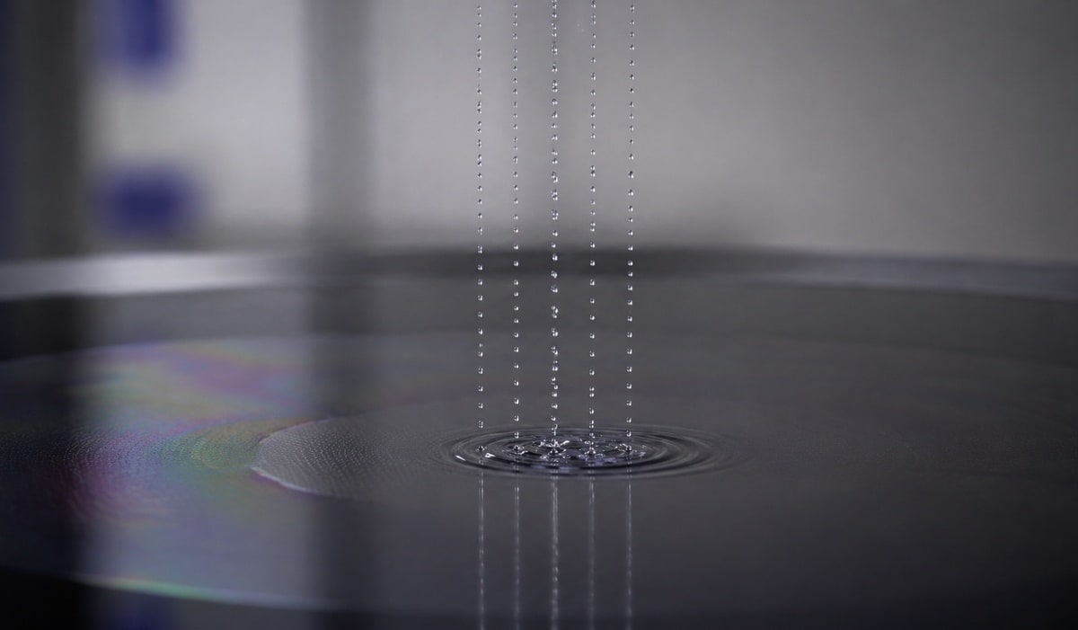
Precision delivery of cleaning chemicals
Frequency control governs droplet size and velocity. This sits alongside ultra-fine laser drilling (Quartz, PEEK) and fluoropolymer bonding (ultrasonic, MVD).
See the products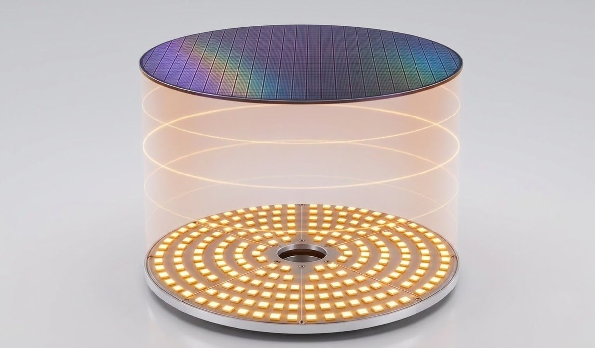
Wafer heating and temperature control
Wafers are heated past 350℃ with centre-to-edge uniformity held within ±3%. Real-time zone feedback control, circuit design and functional testing all run in house.
See the products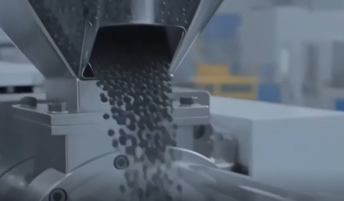
Conductive fluoropolymer
ICP-MS analysis confirms high purity with metal ions under 100 ppb. Carbon brings conductivity below 10³, and the compound stays mouldable to MFR spec.
See the products


IN-HOUSE
process
From R&D and design through machining, assembly, quality verification and delivery, every step runs on our in-house system. Integrated process infrastructure delivers rigorous quality assurance and the best lead time.
Development
DEVELOPMENT
Process
PROCESS
Machining
MANUFACTURING
Assembly
ASSEMBLY
Quality
QUALITY
Delivery
DELIVERY
REVERSE ENGINEERING
process
A reverse-engineering process built on precision 3D measurement and material analysis. Design review, manufacturing and quality verification run one-stop in house, giving a perfect restoration of ultra-fine process parts on the best lead time.
Enquiry received
[Sales]
Design review
[R&D]
Process design and quality criteria
[Production / Process eng.]
Assembly and production
[Manufacturing]
Inspection and certificate
[Quality]
Delivered to the customer
[Sales]

